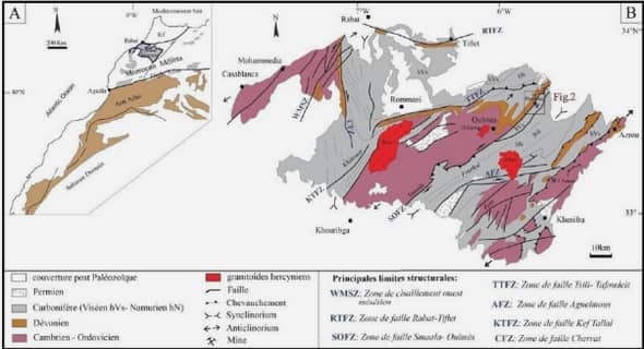
……….
Chapter I: DEEP SUBMICRON MOSFETS
Abstract: The compact modeling of MOS transistors for integrated circuit design has, for many years, been driven by the needs of digital circuit simulation. Conventional bulk CMOS technology is still prevalent in the microelectronics industry. According to the International Technology Roadmap for Semiconductors, bulk MOS transistors will still be used for the 45 nm technology node (gate length around 18 nm), which is expected to be running by 2010.
The feasibility of 15 nm conventional MOS transistors in bulk CMOS technology has already been demonstrated.
The purpose of this chapter is to provide both an overview about the evolution of MOSFETs devices in addition to the basic physics theory required to build compact models required later for the deduction of some mandatory parameters and for the incorporation of new constraints in the function of the device.
I.1. INTRODUCTION
Since the 60’s the shrinking of electronic components has been driven by the fabrication of integrated circuits, which will continue for at least the next two decades. The critical feature size of the elementary devices (physical gate length of the transistors) will drop from 25 nm in 2007 (65 nm technology node) to 5 nm in 2020 (14 nm technology node). In the sub-10 nm range, beyond–CMOS (complementary MOS) devices will certainly play an important role and could be integrated on CMOS platforms in order to pursue integration down to nm structures. Si will remain the main semiconductor material in a foreseeable future, but the needed performance improvements for the end of the ITRS (international technology roadmap for semiconductors) will lead to a substantial enlargement of the number of materials, technologies and device architectures.
………..
![]()