High power amplifiers have been receiving increasing attention as key components responsible for a sizable portion of base station cost in terms of power loss and cooling equipments in wireless communication systems (Jarndal, Aflaki et al. 2010). They are also responsible in large part for battery life and size of the mobile terminals. Thus, high power and high efficiency amplifiers with low power loss are critically needed (Oualid, Slim et al. 2006). To meet these requirements, higher attention should be given to the employed active devices and the circuit design. Today, GaN HEMT devices are the best choice in this regard since they can produce higher output power with lower self-heating and leakage currents, which accordingly results in good power efficiency (Nuttinck, Gebara et al. 2002, Oxley and Uren 2005, Bae, Negra et al. 2007, Milligan, Sheppard et al. 2007, Bensmida, Hammi et al. 2008, Aflaki, Negra et al. 2009, Tanaka, Ueda et al. 2010, Jarndal, Markos et al. 2011). The design of high efficient power amplifier based on AlGaN/GaN HEMT requires an accurate large-signal model for this device (Jarndal, Markos et al. 2011).
The choice of semiconductor materials is based on the physical properties of the materials which have to fulfill the requirements of the application like operating temperature, frequency and bandwidth (Von 2007). Since the power level and the operating frequency of high frequency circuits is steadily increasing, it is predictable that RF power devices based on GaAs will soon come to their performance limitations (Khan, Simin et al. 2005, Nitronex 2009). The most promising materials for high frequency, high power applications are silicon carbide (SiC) and Gallium Nitride (GaN) (Khan, Simin et al. 2005, Von 2007, Yong-Sub and Yoon-Ha 2007).
GaN HEMT semiconductor properties
Gallium Nitride is a wide-bandgap, compound semiconductor that will be a disruptive technology across a wide range of electronic applications (Tanaka, Ueda et al. 2010).Gallium Nitride (GaN) HEMTs (High Electron Mobility Transistors) are the next generation of RF power transistor technology that offers the unique combination of higher power, higher efficiency and wider bandwidth than competing GaAs and Si based technologies (Nitronex 2009).
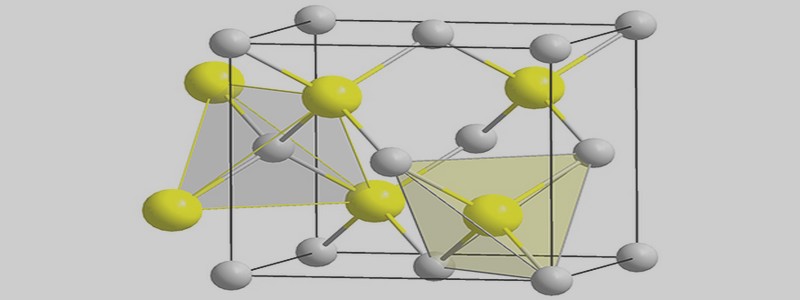
The GaN structure consists of four atoms per unit cell and can be visualized as two interpenetrating hexagonal substructures, one of Ga and one of N atoms related by a spacing u along the c-axis (Komninou, Kioseoglou et al. 2005).
Super material properties for transistors that make them for high power, high energy efficiency and high temperature include wide bandgap energy, high electron mobility and saturation velocity, high sheet carrier concentration at heterojunction interfaces, high breakdown field, and low thermal impedance (Khan, Simin et al. 2005). The bandgap energy is the energy required to ionize atoms and create free electrons. A large bandgap is the key factor for high temperature operation, chemical inertness, and high breakdown voltage.
GaN HEMT growth
The GaN substrates are not a viable alternative for HEMT devices and circuits because of its weak thermal property. Thus, the deposition of GaN thin films on Si and SiC is the primary approach for the fabrication of GaN RF power devices andcircuits. Si substrates have low crystal defect density, zero macro-defects, and offer a high quality surface as required for performing epitaxy (Corporation 2008).
The deposition process is broadly termed as epitaxy and results in a crystalline thin film on the substrate. Metal Organic Chemical Vapor Deposition (MOCVD) is the preferred method of producing GaN-based thin films on Si or SiC for RF applications (Nitronex 2009). MOCVD systems are capable to operate in both conventional and atomic layer deposition regimes (Khan, Simin et al. 2005). Conventional deposition regime wherein precursors enter the growth chamber simultaneously is used to deposit GaN layers. Triethylgallium and ammonia are used as the precursor gases. AlxGa1-xN layers are deposited in atomic layer regime when precursors enter the chamber in a cyclic fashion. Triethylgallium, triethylaluminum and ammonia are used as precursors. The precursors are introduced into the chamber using hydrogen or nitrogen as a carrier gas. Epilayers are deposited on sapphire, Silicon or SiC substrates placed on graphite susceptor, which is heated to the growth temperature by RF-induction.
INTRODUCTION |