Modélisation et optimisation de capteurs de pression piézorésistifs
Phenomenon of the piezoresistivity
Theory
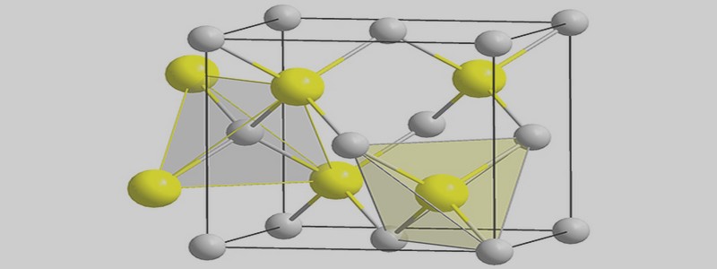
The piezoresistivity phenomenon is not at all a new discovery. If we look back to the history in 1856 Sir Thompson (Lord Kelvin), remarked that the resistance value of metallic bars changes when they are exposed to the mechanical loading. Let us look more carefully at this phenomenon. Basics To start with, let us consider the bar of the unknown material with the spatial dimensions of L, w and t as it is shown in Fig. 2.12. Fig. 2.12 The bar of material under electrical loading. L t w J Modeling and optimization of piezoresistive pressure sensors Michal Olszacki 25 If we force a current flow J, that passes along its length L, through it, we are able to compute its electrical resistance R by using the definition (2.18). wt L R = ρ (2.18) The coefficient ρ is called the resistivity and it is one of the material properties. As one can see, in order to change the electrical resistance, one may perform following actions: change dimension or change the resistivity. What Lord Kelvin did, was the observation of resistance variation of the metallic bars under tensile loading that changes the lateral dimension of the sample (Fig. 2.13). Fig. 2.13 The simplified Lord’s Kelvin experiment. Such a behavior was called the piezoresistance effect. Because, such a kind of transducer transforms mechanical value (strain) into the electrical one (resistance) it is called a strain gauge. In order to compare different gauges or, let us say, different materials, the dimensionless coefficient called the gauge factor was introduced. The gauge factor K is defined as a relative change of resistance to the applied strain ratio (2.19). L / L R / R K ∆ ∆ = (2.19) One of the pioneers that started to use the metallic strain gauges in metrology was Bridgman in 1932 . He experimented with different materials and he has been looking for the one with the highest gauge factor. Unfortunately, in case of metals or their alloys, gauge factors are relatively weak (2 to 4) and thus, the useful output signal is hard to detect. In fact for the metallic strain gauges, the piezoresistive effect appears mostly due to the dimension changes not to the change in the resistivity parameter. It was reported by Bridgman as the following relation (2.20). The C is called the Bridgeman constant whereas V is the volume of the sample. Smith’s discovery The real milestone in the history was the discovery of the piezoresistive effect in silicon by Smith in 1954 [33]. Silicon in the fifties was very promising material since microelectronics technology has became more and more mature those days and thus, a lot of work has been done in order to characterize it. Smith presented the results of studies on both N and P type silicon and Germanium samples and estimated piezoresistive coefficients. Amazingly, those first results showed that the estimated possible gauge factors are about 30 times higher comparing to those that were achieved in metallic gauges. It is caused by the fact, that in silicon, the resistance change is caused mainly by the resistivity then dimensions variation. Thus, it is called the piezoresistive effect. It showed that silicon is the material that not only may be used as a semiconductor to produce new electronic devices such as transistors, but it also offers excellent sensing possibilities. Three years later (1957), Mason and Thurston [34] presented the result of study on possible application of the piezoresistive effect in silicon based force sensors; it took a four years when in 1961 Pfann and Thurston [35] presented the first working device. Another important date was the year 1963 when Tufte and Stelzer [36], followed by Kerr and Milnes [37] published their studies on dependence of the piezoresistance coefficient on temperature, doping level and the crystallographic orientation.
Modeling
Let us consider again, the bar of material under tensile loading (Fig. 2.13). As we know from the previous part of this chapter, each element of the cubic shape crystal will be exposed to normal and shear stresses (Fig. 2.8). It was mentioned that there are two components that may change the electrical resistance value: resistivity and geometrical dimensions. Unlike in metallic bars, in silicon the variation of resistance is in 99% due to the resistivity change than the geometry change and thus, for all calculations we will neglect the second source of the piezoresistive effect. Assuming additionally small stresses and thus, small deformations of the crystal lattice, if we consider the isotropic material, the piezoresistance effect may be expressed by the equation 2.21, where ρ is the resistivity, ρ0 is the resistivity value for unstressed sample, σ is an induced stress value and π is called the piezoresistance coefficient. ρ = ρ0 + ρ0πσ (2.21) Modeling and optimization of piezoresistive pressure sensors Michal Olszacki 27 Introducing a more general approach for the anisotropic diamond-like structure of silicon, we may apply analogous description as it was used in case of the mechanical behavior. Let us then to formulate an Ohms law (2.22) for the three dimensional, cubic element of the Silicon (Fig. 2.13) which is exposed to the vector E of the electrical field that stimulates the current flow defined as a vector J. In case of the silicon structure there is again some symmetry that may reduce the piezoresistivity tensor to the six elements. Moreover, for unstressed silicon, only the diagonal elements of the sensor (ρxx, ρyy, ρzz) will have the nonzero values and will have an equal value ρ, so if we apply again the conversion (2.7), the tensor ρ may be rewritten as follows . Finally, it lead us to the final form of the equation that describes the relation between the stress and resistivity for anisotropic silicon crystal .) Three coefficients π11, π12 and π44 describe completely the piezoresistive behavior of the anisotropic material with diamond-like crystal lattice. Their values were experimentally estimated by Smith for the low doped silicon, both N and P type (Table 2.4).
1 Introduction |