Évaluation et pilotage des activités de recherche dans la R&D centrale de STMicroelectronics
RESULTS: UNCOVERING A NEW FORM OF AC IN RADICAL INNOVATION SITUATIONS
In presenting the findings we first provide brief descriptions of the cases. We follow this by analyzing each case, utilizing the major research questions of our study.
Image sensors at STMicroelectronics
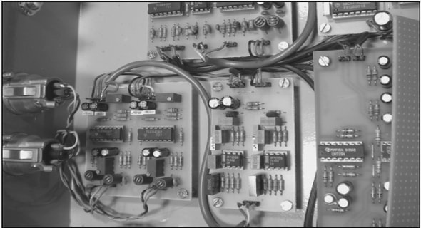
One of the major businesses of STmicroelectronics is the design and manufacturing of image sensors, one of the main building blocks in a digital imaging system such as digital still or video camera. The market for image sensors has been experiencing explosive growth in recent years due to the increasing demands of mobile imaging, digital still and video cameras, internet-based video conferencing, surveillance and biometrics. With over three hundred million parts shipped in 2007 and an annual growth rate over 25%, image sensors have become a significant silicon technology driver. The image sensor became a central business for STMicroelectronics almost ten years ago when it became possible to build low-cost image sensors on the basis of the classical technologies used for microprocessors (CMOS technologies), thus creating a market of cameras for the mobile phone. Just as the microprocessor industry follows the Moore’s law, every two years for the last ten years the CMOS image sensor industry has developed a new generation of products that improves the sensor resolution by reducing the size of each individual pixel that composes an image sensor. But each surface reduction tends to decrease the performance of the single pixel, since each one receives less light. Therefore one of the main challenges consists in shrinking the pixel size without decreasing the pixel performances. To meet the challenges of designing the next generations, several innovation projects are launched ranging from classical improvement to more discontinuous projects. At ST two types of projects are clearly distinguished. D-projects (development projects) are optimizing existing architectures to get the required performance for the very next generation. Advanced R&D (ARD) projects are in charge of exploring the ways to get radical enhancement of the imager through breakthroughs in architectures and processes. On imagers, the two types of projects are very different in size: D-team gather 15 to 20 people (full time job) per year vs. 1 to 3 people (full time job) per year on ARD projects. We followed the D and ARD projects on the development of the next image sensor generations during the period from end 2005 to 2008. D projects are: the so-called 175-generation (launched in 2007), the four “grades” projects in this generation (i.e. projects to improve the 175 generation), three “experts” 115 projects in charge of developing expertise for the generation and the development project for the following generation (so-called 140-generation). There was one ARD team in charge of exploring alternate concepts for the following generations, working from 2005 to 2009. D-teams perform very well since ST was able to stay on the roadmap and propose the right generations of product in the period. ARD teams perform also well since ST was among the first to present breakthrough prototypes of rule-breaking technologies (second in backside1 prototypes, first in 3D prototype). In such a science based industry, all teams exhibit some absorptive capacity, i.e a capacity to make efficient use of external knowledge. In semiconductor industry the external milieu provides a lot of knowledge through publications, conferences, etc. Hence STMicroelectronics teams are supposed to make use of the knowledge provided by external research labs, suppliers, customers, competitors, etc. We compared how D-teams and ARD teams make use of external knowledge.
Observations
We develop each facet of conceptual absorptive capacity in detail next. For each we study the classical aspects of absorptive capacity: 1) the role of prior related knowledge, considered as one major determinant of AC in EAC models 2) the role of strategic vision, organization and mental models, which are considered as moderators (control variables) in EAC models 3) the effect of each facet on the use of external knowledge for radical innovation. For each we compare the case of interest with the reference to ensure that the facet is a characteristic feature of a new type of AC, different from the classical EAC. We evaluate the effect of the facet on AC and the radical innovation output.
Rule-breaking capacity
In radical innovation situation, ARD teams designers at ST face an ambiguous situation where there is a lot of knowledge available to work on their project (scientific, technological, business knowledge,…) but they feel that using directly this knowledge is very likely to impede radical innovation. Our data suggest that designers in such situations actually organize to break design rules to avoid the immediate reuse of existing knowledge. This is a clear difference with classical AC in incremental situation. The C-K representation of these different design trajectories is given in figure 4.People in charge of designing the next (D-teams) make immediately hypotheses on the knowledge they will use: they keep CMOS technologies, which is the mainstream technology used for transistors, following the Moore’s law; they try to adapt and optimize the CMOS technology to an image sensor while keeping changes to CMOS as low as possible. The projects in D feasible target for performance improvement. They are compulsory based on CMOS architectures and technologies imagers (based on electronic on CMOS and optic on CMOS). The projects show a strong AC: they use externally produced knowledge on CMOS, either knowledge coming from CMOS manufacturing, CMOS suppliers, knowledge on optic on CMOS (also suppliers and research labs). Our observation on D-teams fit with the classical pattern of absorptive capacity: the interviewees explain they use CMOS knowledge) that this knowledge base is very likely to help them get the image sensor performance. They also know how to use CMOS image sensors. Moreover they know the next gener law. Hence they know how to make use of knowledge appears as one major determinant of AC in D of AC are also confirmed: the interview that the imager business profitability approximately since its creation is linked to the capacity to use CMOS-based knowledge (and related manufacturing capacities). Hence the use of CMOS knowledge actually relies on a debate on the use of CMOS: the investments are high but considered as justified (unavoidable) in the imager business. The competition is said to follow the same strategic path, as it is known through conferences, through customer roadmaps (mobile phone makers), patents, research programs and PhD dissertations. Figure 4 : D and ARD team design trajectory People in charge of designing the next generation of image sensor in a incremental mode teams) make immediately hypotheses on the knowledge they will use: they keep CMOS technologies, which is the mainstream technology used for transistors, following the Moore’s timize the CMOS technology to an image sensor while keeping changes to CMOS as low as possible. The projects in D-teams have a clear, predictable, feasible target for performance improvement. They are compulsory based on CMOS architectures and technologies. They use competences derived from past generations of imagers (based on electronic on CMOS and optic on CMOS). The projects show a strong AC: they use externally produced knowledge on CMOS, either knowledge coming from CMOS manufacturing, CMOS suppliers, CMOS research labs; they also use externally produced knowledge on optic on CMOS (also suppliers and research labs). teams fit with the classical pattern of absorptive capacity: the interviewees explain they use CMOS-related knowledge because they know (prior related knowledge) that this knowledge base is very likely to help them get the image sensor performance. They also know how to use CMOS-related knowledge in the specific context of image sensors. Moreover they know the next generations of CMOS, which follow Moore’s law. Hence they know how to make use of external knowledge on image sensors. Prior related knowledge appears as one major determinant of AC in D-teams. The “internal” determinants of AC are also confirmed: the interviewees and the heads of image sensors division consider that the imager business profitability approximately since its creation is linked to the capacity based knowledge (and related manufacturing capacities). Hence the use of lly relies on a widely shared mental model. There is no strategic debate on the use of CMOS: the investments are high but considered as justified (unavoidable) in the imager business. The competition is said to follow the same strategic n through conferences, through customer roadmaps (mobile phone makers), patents, research programs and PhD dissertations.
Hook building through generative models
Once basic design rules are broken, classical accesses to external knowledge are not available anymore while links to new knowledge bases are not built. For instance breaking the rule “based on CMOS” free from CMOS constraints and cut from CMOS knowledge base but does not clarify the competences that should be activated. Our data suggest that designers work to counterbalance these consequences of the “rule-breaking” capacity by linking their innovative (rule-breaking) project to external knowledge bases. They build “hooks” to attract external knowledge to their innovative projects. Each hook appear as one specific “problem space”, with more clearly identified “fitness function”, “constraints” and search process. Each single problem space paves the way to the use of a new “epistemic AC”. But to keep the advantage of being free from the fixation effect induced by design rules, designers generate not only one problem space but several problem spaces derived from the rule-breaking project. Hook building is hence a capacity to use existing external knowledge in rule-breaking innovation situations. In ARD teams, rule-breaking led to generate several alternatives to the “CMOS-based pixel” in a rigorous way. How are they generated? The experts explained that these paths were generated by using what they call “a simple model” on “how to get a (Si)-layer for a photodiode on the top of the image sensor pixel?”. This requires a technical explanation: one of the advantages of using CMOS-based pixel is that the Si-wafer is used as a photoelectric surface (it plays the role of a photodiode that “transforms” photonic signal into electronic signal). This SI-layer is provided “for free” (since the wafer is the basic of the whole component). Not driven by keeping CMOS, designer wonders what is the best way to “create” or “find” a layer and where this layer should be ideally. Ideally the photodiode should be directly to the light and as large as possible to get as many photons (as much light) as possible. Hence the question. With this question they generated three main alternatives: the so-called “backside” consists in keeping the existing pixel and turning it upside down, so that Rulebreaking Analysis of the EAC reference Analysis in CAC Phenomenon (no rule breaking: in EAC, follow the “DNA” of the family of products) Break a particularly constraining design rules, offering promising alternatives. “Unlearning” Prior related knowledge Prior related knowledge gives the design rules to be applied, defines the problem space and gives the probability that a solution will be found in that problem space Prior related knowledge helps to identify the “most constraining / most “promising” design rule, occasionally through specific investigations Strategy, mental models and organization The design rules are coherent with organization, strategy and mental models. Strategy: desorptive capacity corresponds to a “strategy to change”. Rule breaking is seen as a “careful alternative”, as a “complementary” alternative. Mental models: wish to make mental models evolve Organization: based on “organized deviance”. There is a true organizational support with a mission to change the game (even if it is with limited resources). Effect on AC Directly linked to a community that provides relevant knowledge for exploring the problem space. Cut from classical knowledge providers. Sensitive to “out of the box” signals (so called weak signals) Effect for innovation Quick identification of a relevant problem space Capacity to resist fixation effect: avoid to be fixed by the design rule light enters through the “backside” of the CMOS consists in building a Si-layer on the top of transistors; the 3D alternative consists in building transistors on the top of a photodiode and turning the whole upside down are not solutions for the ideal pixel, they are just “design paths”, generated model of pixel architecture. Each path defines a problem space with specific fitness functions, constraints and related knowledge domains on “turning upside down” which means actually cutt contact research labs specialized in material handling whereas above IC will focus on how to build a “hot” Si-layer on a “fragile” metal layer and leads to research labs and process experts working on “low temperature” S The C-K representation of this phase of the ARD design trajectory is depicted in Figure Figure 5 : The generative model appears in K (“Si in C (“backside”,…) which conversely lead to explore internal and then external K on We can clearly differentiate this process from the classical EAC in D rule acceptance, D-teams identify one main problem space and Design rules help to frame the problem; they also help to subdivide it into sub problem spaces, in a classical WBS (work breakdown structure). For instance the improvement of 175 generation took the form of a series of rul (grades 1 to 6) AC at each stage favors a wide, efficient exploration of the whole problem space: bringing more detailed expertise, AC helps to counterbalance a kind of “bounded rationality” that prevents designers to really find the optimum in the problem space. enters through the “backside” of the CMOS-based pixel. The “above IC” alternative layer on the top of transistors; the 3D alternative consists in building transistors on the top of a photodiode and turning the whole upside down. T for the ideal pixel, they are just “design paths”, generated model of pixel architecture. Each path defines a problem space with specific fitness functions, constraints and related knowledge domains. For instance the backside pixel path leads to work on “turning upside down” which means actually cutting and bonding wafers and leads to contact research labs specialized in material handling whereas above IC will focus on how to layer on a “fragile” metal layer and leads to research labs and process experts working on “low temperature” Si-layer. K representation of this phase of the ARD design trajectory is depicted in Figure : Hook buildingthrough generative models. The generative model appears in K (“Si-layer = deposition?…”). It leads to create “hooks” (“backside”,…) which conversely lead to explore internal and then external K on focused topics (“SOI”,…) We can clearly differentiate this process from the classical EAC in D-teams: after design teams identify one main problem space and organize a search process in it. Design rules help to frame the problem; they also help to subdivide it into sub problem spaces, in a classical WBS (work breakdown structure). For instance the improvement of 175 generation took the form of a series of rule-based design projects with well AC at each stage favors a wide, efficient exploration of the whole problem space: bringing more detailed expertise, AC helps to counterbalance a kind of “bounded s designers to really find the optimum in the problem space.
Pourquoi les enjeux de l’innovation de rupture dans les semi-conducteurs amènent à reprendre la question de l’évaluation de la recherche ? |